When two unique insulating materials are layered one on top of the other in a “sandwich,” something truly unexpected can occur: A very thin “filling” may appear at the interface between them that is able to conduct electricity. That conducting interface makes this sandwich, known by the combined abbreviations of its two layers – LAO/STO – the focus of a great deal of research. Among other things, this interface has unusual properties that hint at possible uses in new types of electronics. But because the conducting electrons are buried beneath the surface, tightly confined within the sandwich, it has been difficult to understand how the electronic phenomenon takes place, especially on the microscopic level.
Now, researchers in the Weizmann Institute’s Condensed Matter Physics Department have created a sensor that can see through the top layer of an insulating material to reveal how the electrons behave deep inside.
Their findings, which recently appeared in
Nature Materials, reveal that the physics of the LAO/STO interface is much richer in its microscopic structures than scientists had previously thought.
The sensor was created by
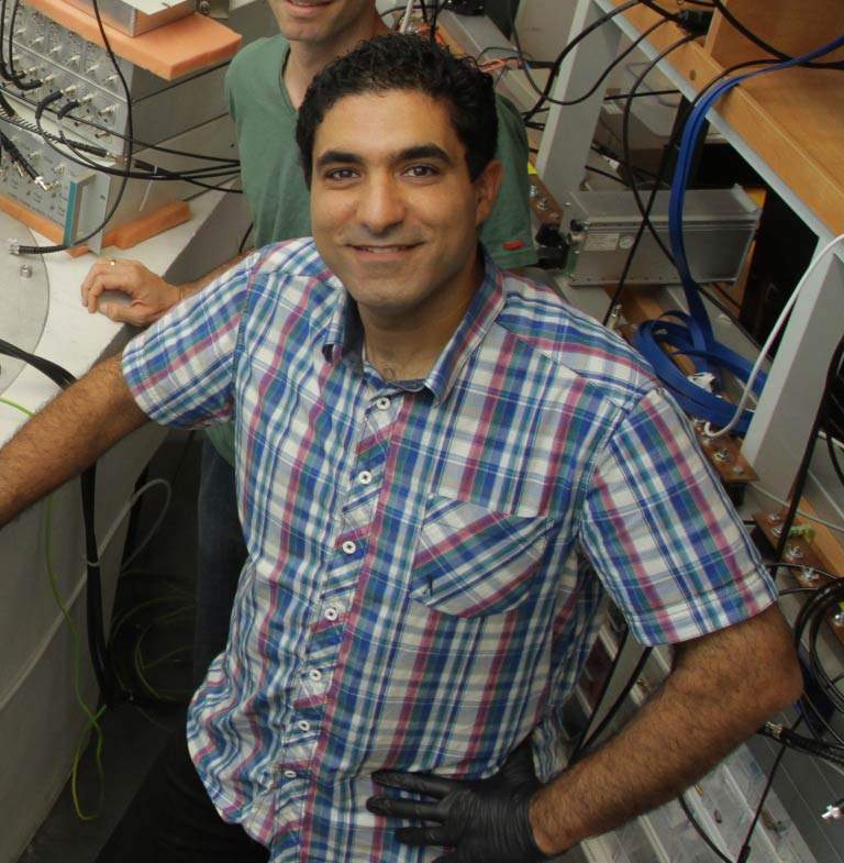
Dr. Shahal Ilani and his team using a nanoassembly technique they had previously developed for making new types of electronic devices based on single carbon nanotubes. The team first employed their pristine nanotubes in complex electronic devices to study the physics of electrons and phonons on the nanoscale. The exceptional behavior of these devices led them to realize, however, that they could also be used as ultrasensitive, nanometer resolution detectors for electric fields.
Ilani, research student Maayan Honig and postdoctoral fellow Dr. Joseph Sulpizio, in collaboration with
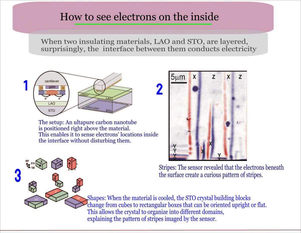
Prof. Eli Zeldov's group of the same department, used this novel sensor to investigate the electric fields in LAO/STO that had been cooled down to very low temperatures – in the range in which many exciting physical phenomena appear. The sensor – a pristine nanotube with an electrical current flowing through it that is extremely sensitive to nearby electric fields – was positioned to hover directly above the LAO/STO sandwich.
Unlike other nanoscale probes, their sensor did not actually touch the surface or transfer current to the material under investigation, ensuring that the technique would not interfere with any process occurring in the LAO/STO. Using the sensor to scan across the surface as they applied different electrical perturbations to the sandwich, they were able to image the physics of the buried conducting layer.
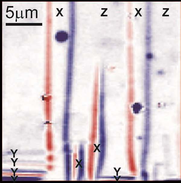
The team was excited to find that their setup did indeed grant them a clear, “x-ray-like” view beneath the surface of the material. But bigger surprises were in store. For one thing, they found that the upper surface of the material moved up and down to an extraordinary extent in response to the applied voltage. This so-called piezo response was known from other materials but was not expected to be significant in LAO/STO. Even more surprising was the discovery of a clear pattern of stripes bearing a strong electrical fingerprint distributed throughout the interface.
According to the researchers, the explanations for both the stripes and the movement lie in the crystal structure of the STO, the bottom half of the sandwich. At low temperatures, the STO crystal breaks its rotational symmetry: Instead of the perfect cubic form it has at higher temperatures, it takes on elongated, rectangular shapes that can lie either parallel to the surface or perpendicular to it. These two orientations form microscopic domains that are ordered in a “comb” of alternating stripes. An applied voltage flips vertically oriented domains to lie horizontally, changing the landscape of the striped domains. This microscopic rearrangement inside the STO is responsible for the anomalously large piezoresponse they observed.
Those striped domains dramatically affect the way electrons flow through the interface, squeezing them into narrow channels. This finding was supported by recent independent experiments at Stanford University which showed that the electrical current indeed travels along narrow paths rather than flowing uniformly throughout the entire interface. These findings are extremely important for understanding the physics of these curious interfaces.
The stripes may have special relevance for the future of nanotechnology. On the one hand, those who want to develop LAO/STO-based electronics will need to find ways to control these stripes. On the other hand, the narrow stripes could give rise to new types of electronics not yet imagined. Sulpizio: “The current in the two-dimensional interface may be compressed into one-dimensional ‘wires’ at the boundaries between stripes. Any time you change dimensions, you are likely to see new physics emerging.”
In the meantime, Ilani and his group are continuing to refine their nanotube sensor, aiming to exploit it as a powerful, nanoscale imaging tool for a growing class of useful quantum materials. Such materials will be central to future technological breakthroughs, as well as offering a gateway to the discovery of new phenomena in fundamental physics.
Dr. Shahal Ilani's research is supported by the European Research Council. Dr. Ilani is the incumbent of the William Z. and Eda Bess Novick Career Development Chair.
Prof. Eli Zeldov's research is supported by the Carolito Stiftung; and the European Research Council. Prof. Zeldov is the incumbent of the David and Inez Myers Professorial Chair.


